
Dia 1 Segunda-feira, 22 de junho
-
18:00|
Receção de boas-vindas



Tópicos abordados
IA para o design de circuitos integrados analógicos/digitais | Aprendizagem automática para EDA | Aceleradores de hardware para IA | Computação neuromórfica | Automação de design
Aprendizagens
No final do programa, os participantes terão adquirido uma compreensão abrangente de como a IA está a alterar fundamentalmente o panorama do design de circuitos integrados. Os participantes vão interagir diretamente com ferramentas e metodologias de última geração, aprendendo a aplicar aprendizagem automática e modelos generativos a fluxos de design do mundo real. O programa proporciona contacto direto com os desafios atuais na indústria dos semicondutores, enquadrando-os através da perspetiva daqueles que os resolvem. Em última análise, a escola serve como um centro colaborativo, oferecendo uma oportunidade única de estabelecer contactos com especialistas de renome e construir redes profissionais valiosas para uma carreira na vanguarda da inovação em silício.
Esta escola de verão explora a poderosa convergência do design de circuitos integrados baseados em IA e o hardware especializado para IA. À medida que os métodos tradicionais de projeto atingem os seus limites, analisamos como a aprendizagem automática está a automatizar o fluxo do projeto – desde o dimensionamento dos circuitos até ao layout - ao mesmo tempo que nos aprofundamos nas arquiteturas de última geração, como chiplets e computação em memória, que impulsionam as cargas de trabalho modernas da IA. Junte-se a especialistas de renome para dominar as ferramentas que estão a redefinir o futuro do setor dos semicondutores.
Através de uma combinação de aulas lecionadas por especialistas e tutoriais técnicos, o programa faz a ponte entre algoritmos teóricos e o silício físico. Irá explorar paradigmas de vanguarda, tais como a integração 3D, a computação fotónica e processamento próximo do sensor, ao mesmo tempo que adquire uma perspetiva holística sobre a forma como estas arquiteturas devem evoluir para responder às exigências de paralelismo maciço e de consumo energético da IA moderna. Ao promover a colaboração interdisciplinar, esta escola de verão equipa-o com os conhecimentos práticos e do pensamento sistémico necessários para contribuir para a próxima geração de sistemas eletrónicos inteligentes.
Nuno Horta (IST/IT) | This tutorial presents a comprehensive overview of the emerging co-design paradigm between Artificial Intelligence (AI) and integrated circuit (IC) design, highlighting their mutually reinforcing relationship. It is structured to provide researchers, engineers, and students with a clear understanding of how AI techniques are transforming IC design methodologies, while advances in IC architectures are enabling increasingly efficient AI computation. The tutorial begins by framing the dual perspective of “AI for IC Design” and “ICs for AI” emphasizing the growing complexity of semiconductor systems and the limitations of traditional electronic design automation (EDA) approaches. The tutorial then traces the evolution of AI in IC design automation, from early optimization-based techniques to modern data-driven approaches. Key applications such as design space exploration, placement and routing, and performance prediction are discussed, showcasing the impact of machine learning in improving efficiency and design quality. A core focus is placed on advanced AI techniques, including deep learning, reinforcement learning, and graph neural networks, and their application to layout analysis, automated floor planning, and circuit modelling. These methods demonstrate significant gains in productivity and the ability to navigate complex design spaces. Shifting to hardware, the need for innovation across both design methodologies and hardware platforms to address the computational demands of modern AI workloads is highlighted. Then, the tutorial explores specialized IC architectures for AI, including domain-specific accelerators and emerging paradigms such as in-memory and neuromorphic computing. It briefly examines critical trade-offs in performance, energy efficiency, and scalability. Finally, the tutorial addresses open challenges and future directions both on AI to IC Design and on IC Design to AI.
Jorge Fernandes (IST / INESC-ID) | Artificial intelligence encompasses a wide range of applications with diverse performance requirements, from high-performance large-scale computing to ultra-low-power edge devices. Across all these domains, energy efficiency remains a fundamental design objective. This talk reviews the evolution of integrated circuits and examines the role of efficient analog and digital circuit design in enabling modern AI systems. It will discuss key design techniques and strategies, from system architecture down to transistor-level implementation, aimed at maximizing energy efficiency. These approaches will be illustrated through representative use cases and practical design examples.
Pedro Figueiredo (Synopsys) | For more than five decades, Moore’s Law shaped the semiconductor industry, delivering predictable exponential gains in performance, density, and cost. Today, a new exponential is emerging: an AI–silicon flywheel in which advances in integrated circuits fuel rapid progress in artificial intelligence, and AI, in turn, accelerates the way we design, verify, and optimise silicon. We examine what AI is providing—or promising to provide—design engineers: reinforcement learning–based optimisation, intelligent copilots, and autonomous agents that augment human expertise, shorten design cycles, and help manage growing system complexity. The talk also addresses the critical role design engineers play in enabling AI at scale by tackling fundamental interconnect bottlenecks in AI data centres. As compute performance continues to outpace data movement, system level constraints are shifting attention to interconnect technologies. High speed SerDes, chip to chip links, and the transition from copper to optical connectivity are becoming decisive factors in shaping performance, energy efficiency, and scalability—and in sustaining the AI–silicon flywheel itself.
Wei-Han Yu (UMacau) | Edge AI chips demand ultra-low power (ULP), compact area, and high efficiency for always-on sensing and inference under strict energy/area constraints. Von Neumann architectures suffer from memory bottlenecks, while digital accelerators and analog compute-in-memory (CIM) face trade-offs in precision, scalability, and leakage. The talk presents a systematic circuit–algorithm co-design framework for area–energy efficient CIM and near-memory computing (NMC), leveraging SRAM bitcells, reconfigurable macros, hybrid analog/digital (A/D) datapaths, and compact neural networks (NNs) optimized for keyword spotting (KWS), speaker verification (SV), vibration-based condition monitoring (VbCM), and ULP feature extraction (FE). We introduce ULP-leakage multi-port SRAM bitcells (5T, 13T) with single-bitline structures, stacked inverters, and power-gating to minimize leakage/read power while supporting in-cell logic and MAC operations. These enable compact CIM macros with high density and robust performance at near-threshold voltages. Reconfigurable, segmented CIM macros support hybrid FP/integer precision, parallel exponent–mantissa computation, and heterogeneous dataflows, reducing external memory access and improving utilization for CNN and Transformer models. Hybrid A/D NMC architectures eliminate high-power ADCs and digital frontends by processing analog features directly, reducing latency and power for always-on sensing. At the algorithm level, we co-optimize NNs with hardware constraints: transfer-computing shares parameters across KWS/SV to halve model size; time-domain extractors adapt to sensor non-idealities to bypass power-hungry FE; and compression modules shrink network size without accuracy loss. The talk highlights how bitcell innovation, reconfigurable CIM, and co-optimization push the frontier of area–energy efficiency for silicon-proven, battery-free IoT and wearable sensors.
Leonel Sousa (IST / INESC-ID) | In recent years, significant research efforts have focused on addressing the exponential growth in computational and memory demands of AI, particularly in deep learning and transformer-based models. This talk presents the latest advances at the hardware level, spanning specialised arithmetic formats, architectures, software frameworks, and full computing systems. We will discuss emerging reduced-precision floating-point and block formats tailored for AI, within the context of the current IEEE working group dedicated to this topic. We will also explore key architectures designed to accelerate AI workloads, with a particular emphasis on matrix–matrix multiplication (MatMul), a core operation underlying most modern accelerators. We will briefly present state-of-the-art systems for both training and inference, including Google's Tensor Processing Units (TPUs), Graphcore's Intelligence Processing Units (IPUs), and Graphics Processing Units (GPUs) equipped with specialised AI hardware. In addition, we will introduce major AI software frameworks, with a focus on PyTorch, and highlight their role in co-design. The final part of the talk will focus on optimisation techniques for embedded inference systems under strict resource constraints. In particular, we will demonstrate the benefits of quantisation and pruning for low-power, resource-limited devices. Finally, we conclude by presenting our experience in developing Processing-in-Memory (PiM) AI accelerators based on ReRAM (Resistive Random Access Memory) technology and their integration into heterogeneous computing systems.
Ricardo Martins - IT / IST | The semiconductor industry increasingly relies on the integration of highly complex systems-on-chip (SoCs), combining analog and radio-frequency (RF) components with multimillion-transistor digital processors and dense memory blocks. Such integration has been made possible by continuous advances in electronic design automation (EDA). However, despite decades of progress, analog design automation still significantly lags behind its digital counterpart. Analog designers and layout engineers continue to rely on traditional environments to manually design and lay out every device and shape in an iterative, error-prone, and difficult-to-reuse process, reflecting negatively in the development and redesign costs of analog and RF blocks. This talk explores the enduring “art” of analog design and the unique challenges that have historically hindered its automation, including design complexity, layout aesthetics, and the strong coupling between electrical and physical implementation. To overcome the limitations of past approaches, the latest solutions—empowered by modern AI techniques—embrace large-scale, holistic optimization frameworks leveraging evolutionary algorithms, machine learning modeling, neural networks, transfer learning, convolutional models, and other emerging techniques. These approaches promise to finally bridge the gap between electrical and physical design, carrying the flow from the netlist to a ready-for-tapeout layout, paving the way for a new era of analog integrated circuit automation.
David Z. Pan (UT Austin) | Designing analog and RF integrated circuits (ICs) has traditionally been a labor-intensive and iterative process, involving manual efforts across circuit topology generation, device sizing, and layout. At every stage, extensive simulations are required to validate performance against design specifications and to optimize circuit behavior. This conventional workflow is not only time-consuming but also lacks scalability. This talk will cover recent advancements in agile and intelligent analog and RF IC design automation, driven by the exponential AI booming. We will showcase AI-driven analog/RF design automation techniques spanning from automated topology generation to device sizing, and to layout synthesis, as well as surrogate modeling and inverse design. We will also present LLM-aided and agentic AI for analog/RF IC design. Our ultimate vision is to enable a fully automated, end-to-end analog/RF IC design flow, from high-level specifications to layout, with or without human in the loop.
Georges Gielen (KU Leuven) | Analog/mixed-signal integrated circuits are key in applications where electronics interface with the physical world. The design of analog circuits, however, is time consuming and prone to errors, often requiring multiple redesign cycles. The rebirth of AI and machine learning, and the recent rise of generative AI methods, on the other hand, create a whole new spectrum of techniques to automate this process. This invited talk will explore the high potential of using advanced machine learning (ML) techniques such as reinforcement learning to automatically synthesize analog integrated circuits. What is hype and what will be feasible? Will we still need analog designers in the future and how will they operate?
David Tournatory (CircuitLeap) | Analog integrated circuit design remains one of the most human intensive disciplines in semiconductors. While digital design has benefited from decades of automation, analog workflows still rely heavily on expert intuition, manual schematic entry, slow CPU based SPICE simulation, and handcrafted layout. The explosive demand for power delivery silicon, driven by AI accelerators, electrification, and edge devices, is exposing the limits of this paradigm. This talk explores how the same GPU hardware that powers modern AI can be turned inward to transform how analog ICs themselves are designed. I will present CircuitLeap's approach to rebuilding the analog design stack around two ideas: GPU native circuit simulation that delivers order of magnitude speedups for power management topologies, and agentic AI that generates and optimizes layout in close collaboration with the designer. I will walk through concrete results on Smart Power Switch architectures, parasitic aware simulation, and automated placement and routing, drawing on real customer deployments in production silicon. Beyond the immediate productivity gains, I will discuss what this shift implies for the future of EDA and for the designers themselves. As AI handles more of the rote work, the role of the analog engineer evolves toward higher level architectural decisions, specification, and verification.

David Tournatory
CircuitLeap

David Z. Pan
UT Austin

Georges Gielen
KU Leuven

Jorge Fernandes
INESC-ID / Instituto Superior Técnico

Leonel Sousa
INESC-ID / Instituto Superior Técnico

Nuno Horta
Instituto Superior Técnico / Instituto de Telecomunicações

Pedro Figueiredo
Synopsys Portugal

Ricardo Martins
Instituto de Telecomunicações / Instituto Superior Técnico

Wei-Han Yu
University of Macau
Esta escola de verão foi concebida para estudantes de mestrado e doutoramento em Engenharia Elétrica e Informática (ECE) e outras áreas estreitamente relacionadas. São bem-vindas as candidaturas de candidatos de outras áreas relevantes. Quer esteja a especializar-se durante o mestrado ou já esteja numa fase avançada da sua investigação de doutoramento, o programa oferece a profundidade técnica e o contexto industrial necessários para colmatar a lacuna entre os estudos académicos e os mais recentes desenvolvimentos no campo dos semicondutores.
A organização da escola de verão selecionará 50 participantes entre as candidaturas recebidas. Os participantes que frequentarem os três dias da escola de verão receberão um certificado de participação.
É essencial ter proficiência em inglês, uma vez que todas as sessões serão ministradas nesta língua.
Datas importantes:

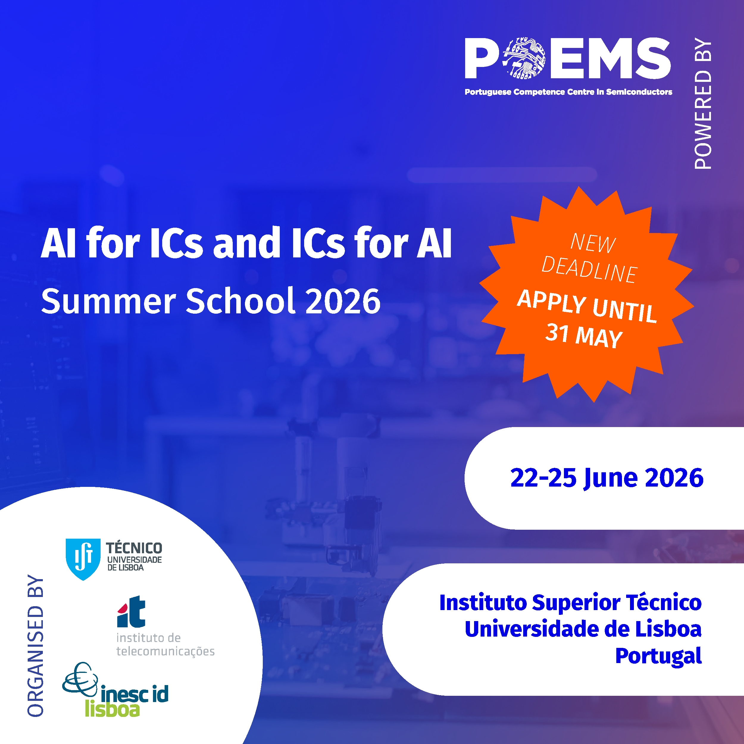
Prazo de candidaturas: 17 de maio de 2026 Novo prazo de candidaturas: 31 de maio de 2026
Notificação de resultados das candidaturas: 20 de maio de 2026
O processo de candidatura decorrerá online, mediante o envio dos seguintes documentos:
Currículo
Carta de motivação
Carta de recomendação (opcional)

O campus universitário fica junto à Alameda Dom Afonso Henriques, em Lisboa.
A localização está bem servida por transportes públicos.

Aulas e materiais fornecidos durante a escola.
Pausas para café, almoços e jantar social (opcional).
O Aeroporto Humberto Delgado de Lisboa fica a cerca de 10–15 minutos do IST.
Lisboa conta com duas grandes estações ferroviárias que servem os comboios Intercidades, Alfa Pendular e internacionais.
Vários autocarros da Carris servem a zona, mas o metro é normalmente a forma mais rápida e prática de se deslocar em Lisboa.
Tenha em atenção que o Instituto Superior Técnico tem duas entradas principais localizadas em lados opostos do campus. Dependendo da estação de metro que utilizar, chegará a um lado diferente:




Comissão organizadora
Fábio Passos( Assistant Professor , Instituto Superior Técnico and INESC-ID)
Nuno Horta(Full Professor, Instituto Superior Técnico and IT)
Ricardo Martins(Assistant Professor, Instituto Superior Técnico and IT)
Jorge Fernandes(Full Professor, Instituto Superior Técnico and INESC-ID)